A team from Peking University has presented a transistor that runs 40% faster than Intel's and TSMC's 3 nm chips, while consuming 10% less energy. The press headlined it "the end of silicon". The paper itself says something more precise and more interesting: it describes a complete architecture, with measured figures, an identified industrial obstacle, and a timeline that nobody cites. Here is what the work actually contains, why the material chosen is no accident, and what it changes — or does not change — for the Western export-control strategy.
- What was announced, and what was published
- The six figures that matter
- Why bismuth, and not another 2D material
- The architecture: GAAFET and monolithic 3D integration
- The misunderstanding: this transistor is not "silicon-free"
- The real obstacle: from laboratory to factory
- The timeline the hype forgets
- What this does to the export-control strategy
- What to take away
1. What was announced, and what was published
The announcement has been circulating for months in a short form: Chinese researchers have supposedly built "the fastest transistor in the world", "without silicon", "40% faster than Intel and TSMC". The headlines are spectacular and, for the most part, accurate on the figures. They are above all incomplete on what matters.
The source is a paper published in Nature Materials, titled "Low-power 2D gate-all-around logics via epitaxial monolithic 3D integration", signed notably by Junchuan Tang, Jianfeng Jiang, Xiaoyin Gao and Xin Gao, with Hailin Peng and Lian-Mao Peng of Peking University as corresponding authors. The title of the paper is itself revealing: it mentions neither speed nor silicon. It speaks of a gate-all-around logic made of a two-dimensional material, obtained by epitaxial monolithic three-dimensional integration.
In other words, the work is not about a miracle material but about a complete chain: how to grow a two-dimensional semiconductor over a large area, how to pair it with a gate insulator without degrading the interface, how to stack several layers, and how to draw working logic gates from it. It is this integration, more than the material itself, that constitutes the result.
The abstract also states the obstacle the authors say they have overcome: at the conceivable angstrom nodes, a gate-all-around architecture based on two-dimensional semiconductors would offer excellent electrostatic control — but "a major obstacle lies in the large-scale integration of gate-all-around 2D heterostructures with atomically smooth and conformal interfaces". The problem was never finding a good material. It was always knowing how to manufacture it cleanly, in volume.
2. The six figures that matter
Here is what the paper measures, on a gate-all-around transistor with a gate length of 30 nanometres.
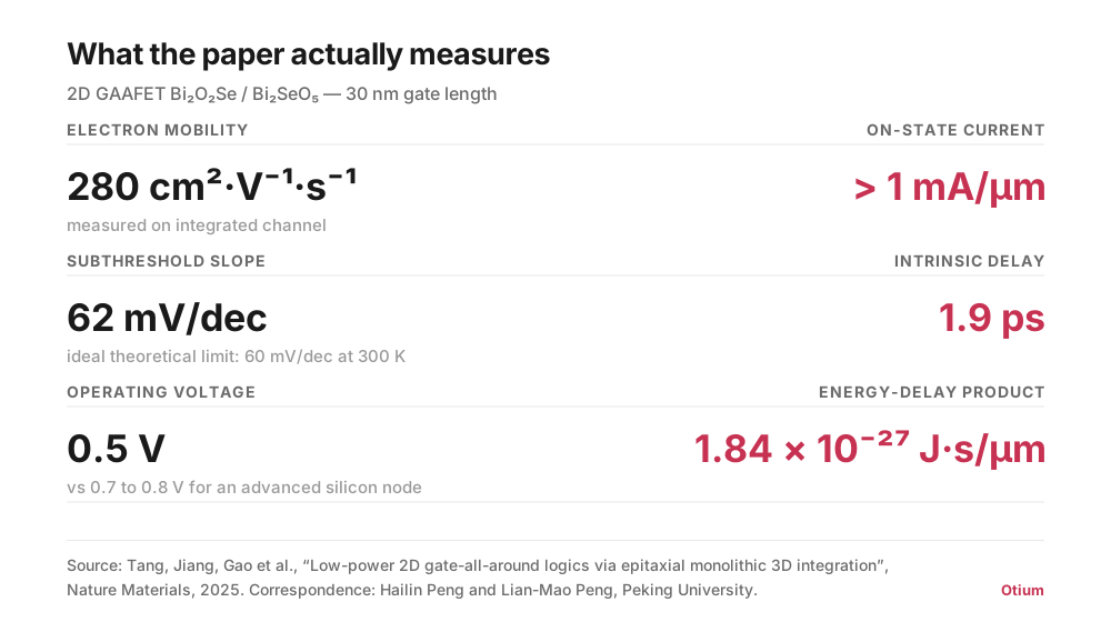
Electron mobility of 280 cm²·V⁻¹·s⁻¹. This is the speed at which electrons move through the channel under the effect of an electric field. The value measured on the integrated device is clearly lower than the ~1,400 cm²·V⁻¹·s⁻¹ observed on isolated Bi₂O₂Se crystals in the laboratory — a normal gap, and an honest one to publish: integrating a material always degrades its raw performance.
Subthreshold swing of 62 mV/decade. This is the most impressive figure of the set, and the least commented on. This quantity measures how effectively the gate controls the opening and closing of the transistor. Physics imposes a theoretical limit of 60 mV/decade at room temperature for a conventional field-effect transistor. Getting 62 means being two units from the ideal. In practice: very little leakage current, and therefore very little energy wasted when the transistor is supposed to be off.
Operating voltage of 0.5 volt. Advanced silicon nodes work rather around 0.7 to 0.8 volt. Yet the energy dissipated varies with the square of the voltage: going from 0.75 to 0.5 volt divides dynamic consumption by more than two, at equal activity. This is where the announced "10% less energy" is decided — and the figure communicated is cautious in the light of the physics.
On-state current above 1 mA/µm. This is the point that gives the work its credibility. The Achilles heel of two-dimensional transistors is precisely here: an atomically thin channel carries little current, and laboratory devices usually compensate by keeping large contact areas — which ruins the miniaturisation being sought. Exceeding a milliampere per micrometre at a 30 nm gate demonstrates that the trade-off has been held.
Intrinsic delay of 1.9 picoseconds and energy-delay product of 1.84 × 10⁻²⁷ J·s/µm. The first measures switching speed, the second combines speed and consumption in a single figure of merit — the only one that allows an honest comparison between technologies. It is from these two values that the "40% faster than 3 nm" comparison derives.

3. Why bismuth, and not another 2D material
Research on two-dimensional semiconductors is nothing new, and candidates are not lacking: molybdenum disulfide, tungsten diselenide, graphene for conduction. The choice of bismuth oxyselenide responds to a precise reason, and it is the intellectual heart of this work.
It is worth recalling here why silicon dominated for sixty years. It is not because it conducts best — gallium arsenide and germanium do better on that count. It is because it has a native oxide: heating it under oxygen yields silicon dioxide, a remarkable gate insulator, chemically bonded to the channel, obtained without depositing a foreign material. This property made all of modern microelectronics. Other semiconductors, lacking a good native oxide, had to resort to added insulators, with defective interfaces that trap charge carriers.
Bi₂O₂Se has exactly this property. Its native oxide, Bi₂SeO₅, is a layered dielectric with high permittivity — what the industry calls a "high-κ" material, precisely what TSMC and Intel obtain today at the price of sophisticated depositions. The Bi₂O₂Se/Bi₂SeO₅ pair therefore reproduces the Si/SiO₂ relationship, but in a two-dimensional version and with an insulator of much better permittivity.
The authors claim an atomically smooth and conformal interface between the two, obtained by epitaxial growth. Density functional theory calculations confirm that this interface has fewer defects and more regular electronic transport than existing semiconductor/oxide interfaces. Added to this are three qualities of Bi₂O₂Se that are rarely found together: air stability — many 2D materials degrade outside a controlled atmosphere —, a bandgap suited to logic, and high mobility.
It is this combination that explains why the specialist literature describes this material as "resembling silicon and its SiO₂". Bi₂O₂Se does not merely reproduce silicon's performance: it reproduces its manufacturability. And in microelectronics, manufacturability almost always beats raw performance.
4. The architecture: GAAFET and monolithic 3D integration
Two technical terms structure the result, and deserve to be translated.
GAAFET, for gate-all-around field-effect transistor: a transistor whose gate completely surrounds the channel. It is the architecture the industry is currently migrating to, after planar transistors and then FinFETs. The more the gate envelops the channel, the better it controls its state, and the less there is leakage. This is what makes continued miniaturisation possible. The Beijing work is presented as the first GAAFET fabricated with a two-dimensional channel — the conjunction of the two, and not each separately, is the novelty.
Low-temperature monolithic three-dimensional integration: instead of manufacturing chips separately and then stacking them, successive layers are built directly on top of one another, in the same process. "Low temperature" is decisive here, because the lower layers must not be damaged during the fabrication of the upper ones. The authors report a single-crystal configuration stacked in several layers, at wafer scale.
This is the point that distinguishes this work from most 2D material demonstrations. The literature in the field abounds in single devices, made by hand on exfoliated flakes, with flattering performance and no industrial future. Here, the scale claimed is that of the whole wafer, with stacking.
5. The misunderstanding: this transistor is not "silicon-free"
This is the soundest criticism levelled at the media coverage of this work, and it comes from industry professionals themselves.
The headline "first silicon-free transistor" describes the channel — the active zone where the electrons flow —, which is indeed made of Bi₂O₂Se. But the device is produced by heteroepitaxy on a silicon wafer. Silicon remains the substrate, the platform, the physical support. Technologies derived from this work would therefore continue to depend on the existing foundries that produce silicon wafers.
The nuance is not cosmetic. It entirely changes the geopolitical reach of the announcement. A process that replaced silicon from end to end would free its holder from the whole current supply chain. A process that adds a layer on a silicon wafer remains dependent on that chain — including the lithography that defines the patterns.
A second point of caution, voiced by sector observers: this is a laboratory chip, not a production chip. TSMC's and Intel's research laboratories work on comparable routes without making press releases about them. Publicly announcing a lead is not, in itself, proof of a lead.
This last argument itself deserves to be put in perspective. In January 2026, imec, ASML and TSMC jointly presented complementary transistors in 2D materials at a 50 nanometre pitch on a 300 millimetre wafer. The Western ecosystem is therefore not absent from the field — it communicates differently.
6. The real obstacle: from laboratory to factory
The specialist literature names precisely what separates this demonstration from industrial production. Three workstreams, listed in the review papers devoted to Bi₂O₂Se.
Material synthesis. Growing high-quality Bi₂O₂Se films over large areas remains difficult, and is the absolute prerequisite for any volume manufacturing. A perfect crystal of a few square micrometres in the laboratory has no industrial value; the same quality is needed across three hundred millimetres of diameter, reproducibly, batch after batch.
Wafer-scale integration. This is precisely what the Beijing work claims to have advanced, and it is why it matters. Parallel publications cover thin Bi₂O₂Se films on insulator for integrated electronics — the subject is active, across several teams.
Contact resistance. This is the dominant obstacle for all 2D transistors, and it is structural: an atomically thin channel carries little current, which laboratory devices compensate for by enlarging the contact areas — cancelling at the same stroke the miniaturisation being sought. Forming low-resistance contacts on two-dimensional semiconductors, and identifying industrialisable gate stacks, remain the two essential requirements for industrialisation. This is where the current above 1 mA/µm reported by the Beijing team takes on its value: it indicates that the trade-off was held on this specific device. It does not say that it will hold in production.
To this list must be added what the publications do not talk about, and which nonetheless decides everything in microelectronics: manufacturing yield. A technology that produces one excellent transistor out of a thousand attempts does not exist industrially. No yield data accompanies this work — which is normal at this stage, and needs to be said.
7. The timeline the hype forgets
This is the most useful piece of information in this whole file, and the one most absent from the articles that headline the end of silicon.
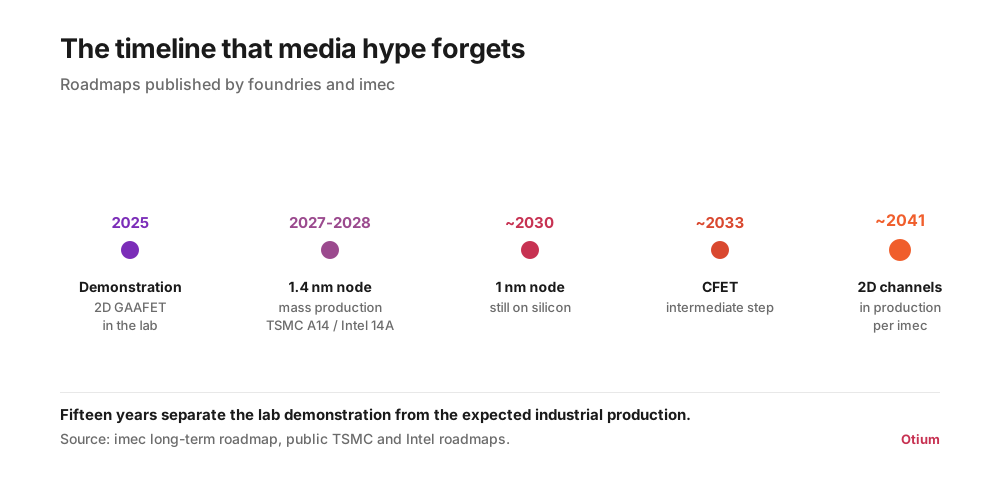
The long-term roadmap of imec — the Belgian research centre that serves as a common reference for the whole industry, including TSMC, Intel and Samsung — places two-dimensional atomic channels beyond 2030, with a shift to 2D semiconductor channels around 2041. In the meantime, the industry plans CFETs around 2033 as an intermediate step.
Until then, it is silicon nodes that advance, and their timetable is public. TSMC (A14) and Intel (14A) have locked in their roadmaps for 1.4 nanometres: pilot production in late 2026 and early 2027, mass production in 2027-2028 for TSMC, with Intel aiming for volume production in 2028. The 1 nanometre node is expected around 2030 — still on silicon.
In other words: between the laboratory demonstration of 2025 and the anticipated industrial production of 2D channels, there are about fifteen years. This is not an objection to the Beijing work — it is the normal pace of microelectronics, where ten to fifteen years usually separate a proof of concept from a production line. The FinFET was proposed in 1998 and industrialised in 2011.
8. What this does to the export-control strategy
That leaves the question that justifies following this subject: how does it alter the technological balance between the United States and China?
The American control regime rests on a simple hypothesis: keep China a few years behind by denying it access to the most advanced machines. In practice, Chinese manufacturers cannot buy ASML's extreme ultraviolet lithography systems and must make do with older deep ultraviolet tools.
This hypothesis was already weakened before bismuth. ASML's chief executive himself has acknowledged that Chinese foundries could reach 7 nm, 5 nm and eventually 3 nm with DUV tools — more slowly, with lower yield and at higher cost, but they can. And the MATCH Act, a bipartisan bill introduced in April, envisages banning ASML from exporting even DUV equipment to China, a sign that Washington has identified the breach.
In parallel, China is building its own tools. Shanghai Yuliangsheng has launched industrial production of DUV immersion lithography machines, with a target of five machines in 2026 and about twenty the following year. The volumes are modest relative to needs, but the trajectory is established.
It is in this context that the bismuth work takes on its real meaning. It is not an immediate workaround — the device is fabricated on a silicon substrate and requires lithography. It is a shift of the competitive terrain. Export control applies to machines; a lead in materials and in integration processes is not subject to the same regime. A patent does not ship in a container.
Both ends must nevertheless be held. The joint demonstration by imec, ASML and TSMC of complementary 2D transistors at a 50 nm pitch on a 300 mm wafer shows that the Western ecosystem is progressing on the same front, with the decisive advantage of being backed by existing production lines. The passage from laboratory to factory, which is the real obstacle, structurally favours those who already own the factories.
9. What to take away
The result is solid and is worth more than its headline. A team from Peking University has published in Nature Materials a GAAFET with a two-dimensional channel integrated at wafer scale, with a subthreshold swing of 62 mV/decade — two units from the physical limit —, an operating voltage of 0.5 volt and a current above 1 mA/µm. These are measurements, not projections. What is demonstrated is not a miracle material but an integration chain, which is far harder and more useful.
The choice of bismuth is the real stroke of genius. Bi₂O₂Se has a high-permittivity native oxide, Bi₂SeO₅. It thus reproduces the property that made silicon's fortune for sixty years: not performance, but the ability to form a clean interface with no added material. In microelectronics, manufacturability beats raw performance.
"Silicon-free" is false. The channel changes material; the substrate remains silicon, and so does the lithography. Any geopolitical conclusion drawn from the formula is mistaken at the root.
Three obstacles remain, and they are known. Growth of high-quality films over large areas, contact resistance, and — never mentioned in the announcements — manufacturing yield. The third decides everything and is the subject of no published data.
The timeline is fifteen years, not two. imec places 2D channels in production around 2041. Until then, 1.4 nm arrives in 2027-2028 and 1 nm around 2030, on silicon. No investment decision taken this decade should assume anything else.
The subject to watch is not performance, it is the shift of terrain. Western control policy applies to exportable machines. A lead in materials and integration processes escapes that instrument. If the next decade is played out on interface chemistry rather than on optical precision, the current main regulatory tool will progressively become pointless — and this shift will not announce itself, it will be noticed after the fact.